In the realm of modern technology, the search for high-performance materials with tailored properties is crucial. Thin films have emerged as a vital component in various industries, from semiconductors to optical coatings, offering precise control over their properties. DC sputtering, a remarkable technique, enables the deposition of thin films with exceptional accuracy. Whether you’re a researcher, engineer, or simply curious about material coatings, this guide equips you with the knowledge to understand, utilise, and innovate in thin film technology.
What is Thin Film Deposition?
Let’s start with the basics. In thin film deposition, a substrate is covered with a layer of material that is only a few nanometers to a few micrometres thick. These tiny films can be found everywhere, from your smartphone’s screen to the protective coating on your car. They play an important role in electronics, photonics, mechanics, and even biomedical applications.
What is DC Sputtering?
One of the various physical vapour deposition (PVD) processes used to produce thin films is direct current (DC) sputtering. Sputtering refers to the ejection of atoms from a solid target material due to energetic particle bombardment. In DC sputtering, a voltage is delivered to a metal target in a low-pressure gas, often an inert gas such as argon. Gas ions clash with the target, “sputtering” off microscopic particles of the target material, which then drop onto a neighbouring substrate.

The Process of DC Sputtering
Now that we know what DC Sputtering is let’s look at the process in detail:
-
Creating a Vacuum
Creating a vacuum inside the process chamber is the first step in the DC sputtering process. This isn’t just for cleanliness (though that is a consideration). Having a vacuum available aids in process control. In a low-pressure environment, the mean free path significantly lengthens. This is the average distance a particle can travel before colliding with another. This permits the sputtered atoms to go from the target to the substrate without interacting with other atoms, resulting in a more uniform and smoother deposition.
-
Introducing Inert Gas
After the vacuum is established, an inert gas (usually argon) is introduced into the chamber. The pressure of the gas is kept low, usually a few milliTorr. The use of an inert gas is intentional. We don’t want the gas atoms to react with the target material or the substrate; we only want them to provide a medium for the plasma to form.
-
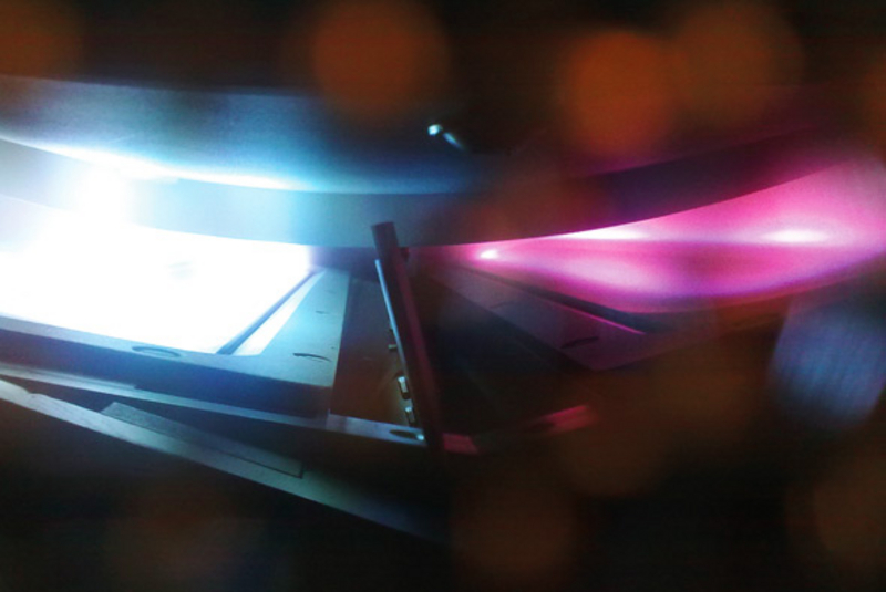
Igniting Plasma
A voltage applied across the target and the substrate ionises the argon atoms, forming a plasma. Plasma is essentially a soup of positively charged ions and free electrons. In the case of direct current sputtering, electrons are brought to the anode, whereas positive ions are drawn to the cathode, which is the target.
-
Sputtering the Target
When positive ions collide with the target, they knock off (or sputter) atoms from the substance. The ion energy and the mass of the target atoms determine the amount of material spat off. This is why the process tightly manages to ensure a consistent sputtering rate.
-
Thin Film Deposition
Finally, the sputtered atoms traverse the chamber and land on the substrate. Because of the low pressure and the sputtered material’s characteristics, these atoms tend to deposit highly uniformly, resulting in a thin coating of consistent thickness.
Considerations and Limitations in DC Sputtering
DC Sputtering is not without difficulties. For example, it is not ideal for insulating materials because they can build charge and interrupt the sputtering process. Accurate regulation of process factors such as gas pressure, target-substrate distance, and voltage is necessary for achieving the best results.
DC Sputtering vs RF Sputtering
While DC Sputtering offers advantages, Radio Frequency (RF) Sputtering is another technology commonly employed for insulating materials that overcomes one of DC Sputtering’s shortcomings. RF Sputtering uses an alternating current to prevent charge buildup on the target, allowing it to effectively sputter insulating materials.
Advantages of DC Sputtering
DC sputtering offers five main benefits in thin film deposition:
Precise Control: DC sputtering enables precise control over the deposition process, allowing for tailored thickness, composition, and structure of thin films. This ensures consistent and reproducible results.
Versatility: DC sputtering applies to many fields since it may deposit many different substances. It’s useful for various materials, including metals, alloys, oxides, nitrides, and more.
High-Quality Films: DC sputtering produces high-quality thin films with excellent adhesion to the substrate. This results in uniform coatings with minimal defects and impurities, ensuring desired performance characteristics.
Scalability: DC sputtering is a scalable technique suitable for large-scale industrial production. It can deposit thin films over large areas, meeting high-volume demands efficiently.
Energy Efficiency: DC sputtering is relatively energy-efficient compared to other deposition methods. It utilises a low-pressure environment and requires lower power consumption, leading to cost savings and reduced environmental impact.

Emerging Trends in DC Sputtering
Technology never stands still, and DC Sputtering is no exception. We can expect more efficient processes and superior thin film quality with advancements like High Power Impulse Magnetron Sputtering (HiPIMS). HiPIMS provides excellent film density and smoothness and enables the deposition of insulating materials, thus overcoming the limitations of traditional DC Sputtering.
Moreover, the increasing interest in two-dimensional (2D) materials like graphene for electronics, photonics, and energy storage applications has led to new research avenues for DC Sputtering. The potential for developing these 2D films using sputtering methods is an exciting frontier in thin film deposition research.
Wrapping Up
DC Sputtering has proven to be a versatile and reliable method for thin film deposition, with its foothold in various industries. As the demand for thin films grows, so will the techniques and technologies involved in their production. As we move towards an era of miniaturisation and higher efficiency, the role of DC Sputtering in shaping our future cannot be overstated.
The thin film technology, and DC Sputtering as a part of it, will continue to evolve, revolutionising numerous applications ranging from solar cells to computer chips. Because of its versatility, scalability, and ability to deposit a wide range of materials, it will continue at the forefront of thin film deposition. This will enable improvements in electronics, optics, energy, and beyond.